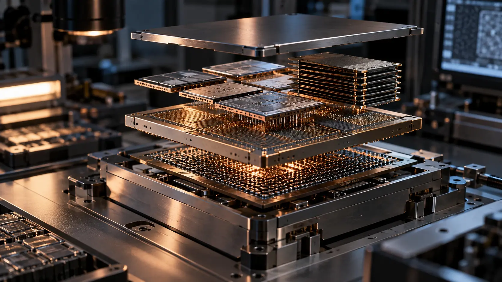
Chiplet technology and 3D chip stacking are changing the way advanced processors are designed. Instead of building every function on one large piece of silicon, manufacturers can divide a system into smaller components and then connect them inside the same package. Some designs place these components side by side, while others stack them vertically. The result is a more modular approach to semiconductor design that can improve performance, increase manufacturing flexibility, and reduce some of the costs associated with producing very large chips.
Traditional processors are often built as monolithic dies, meaning most of the major functions are fabricated together on a single piece of silicon. This approach has important advantages, especially because communication within one die can be fast and efficient. However, as processors become larger and more complex, monolithic designs become increasingly difficult and expensive to manufacture. A single defect can make a large die unusable, and producing every part of the chip on the most advanced manufacturing process may not be economically sensible.
Chiplets address this problem by dividing a processor into smaller dies that can be manufactured separately and then assembled into a larger system. One chiplet might contain CPU cores, another could handle input and output, and others could provide graphics, memory control, artificial intelligence acceleration, or specialized functions. These chiplets communicate through high-speed links inside the package, allowing them to behave as parts of a unified processor.
This modular structure offers a major manufacturing advantage. Smaller dies generally have better production yields because there is less area in which a defect can occur. If a large monolithic processor contains a flaw, the entire chip may need to be discarded. With chiplets, manufacturers can test individual components before assembly and use only the ones that meet quality requirements.
Chiplets also allow different parts of a system to use different manufacturing technologies. High-performance compute cores may benefit from the newest and most expensive process node, while input-output circuits, cache, analog components, or other functions may work perfectly well on older and cheaper processes. Instead of forcing every part of the processor onto the same technology, designers can select the most appropriate process for each component.
This flexibility can reduce cost while also improving product development. A company may be able to reuse the same compute chiplet across several processors and combine it with different memory, graphics, or connectivity components. That makes it easier to create multiple products without redesigning the entire chip from the beginning.
The approach also supports specialization. Modern computing systems increasingly combine different types of processors because no single architecture is ideal for every workload. CPUs are well suited to general-purpose tasks, GPUs excel at highly parallel computation, and dedicated AI accelerators can perform neural-network operations efficiently. Chiplet-based systems can bring these functions together more easily within one package.
The challenge is communication. When components are separated into different dies, information must cross physical interfaces between them. These connections can introduce latency, consume energy, and limit bandwidth. If communication is too slow, the benefits of modular design can be reduced. High-speed interconnect technology is therefore one of the most important parts of chiplet architecture.
Advanced semiconductor packaging helps solve this problem by placing chiplets extremely close together and providing dense electrical connections between them. Some packages use silicon interposers, bridges, or other structures that create high-bandwidth links across short distances. The closer and denser these connections become, the more the chiplets can behave like components of a single larger processor.
Standards are also becoming important. If chiplets from different designers are expected to work together, they need compatible physical and communication interfaces. Industry efforts toward standardized die-to-die interconnects could eventually make chiplets more interchangeable, creating something closer to a modular ecosystem for semiconductor design. This could allow companies to combine specialized components without developing every part internally.
Three-dimensional stacking extends the same idea into the vertical dimension. Instead of placing components only next to one another, 3D chip stacking places dies or functional layers above and below each other. Electrical connections can run vertically through the stack, dramatically shortening the distance between components.
This can be especially useful for memory. A processor frequently needs to move data between computing units and memory, and this movement can consume significant time and energy. By stacking memory close to processing logic, designers can increase bandwidth and reduce the distance that signals must travel.
High-bandwidth memory is one important example of this approach. Multiple memory layers can be stacked and connected through dense vertical links, creating much higher data-transfer rates than conventional memory located farther away on a circuit board. This has become especially valuable in artificial intelligence and high-performance computing, where processors need constant access to enormous amounts of data.
Three-dimensional integration can also place cache directly above processing cores or combine different types of logic in the same vertical structure. In principle, designers can use the third dimension to increase functional density without relying exclusively on smaller transistors. This is increasingly important as conventional semiconductor scaling becomes more difficult.
Shorter connections can improve energy efficiency as well. Moving data across a large chip or through a circuit board consumes power. If memory and processing components are positioned only a small distance apart, less energy may be required to transfer the same information. Because data movement is a major source of energy consumption in modern processors, this can provide significant benefits.
However, stacking components creates a serious thermal challenge. A flat chip can transfer heat toward a cooling system relatively directly. In a 3D stack, lower layers may be surrounded by other active components, making it more difficult for heat to escape. If several high-power processing layers are stacked together, temperatures can rise quickly.
This limits how aggressively logic can be stacked. Memory generally consumes less power than high-performance compute cores, which is one reason memory-on-logic designs can be attractive. Stacking multiple power-hungry processing dies is more difficult because each layer contributes additional heat.
Thermal management must therefore be considered from the beginning of a 3D design. Engineers may distribute high-power functions strategically, reduce operating voltages, use more efficient cooling technologies, or develop new materials for transferring heat. In some systems, advanced liquid cooling may become necessary as computing density increases.
Mechanical and manufacturing complexity also grows with 3D integration. Layers must be aligned with extreme precision, and the vertical connections between them must be reliable. A defect in one component can affect the entire stack, so testing individual dies before assembly is critical. Manufacturers must also account for stress caused by different materials expanding and contracting as temperatures change.
Packaging has therefore become much more than a final step in chip production. Historically, the package mainly protected the die and connected it to a circuit board. In advanced processors, packaging increasingly determines memory bandwidth, interconnect speed, thermal behavior, and overall system performance. It has become part of the architecture itself.
This shift is closely related to the slowdown of traditional Moore's Law scaling. For decades, much of the semiconductor industry's progress came from making transistors smaller. Smaller transistors allowed more computing capability to fit into the same area. That strategy continues, but it has become increasingly difficult and expensive.
Chiplets and 3D stacking provide another path. Instead of relying only on transistor miniaturization, manufacturers can improve processors by combining multiple pieces of silicon more efficiently. The system can gain more cores, more memory, more specialized accelerators, and faster internal communication even when transistor scaling alone cannot provide the desired improvement.
Artificial intelligence is one of the strongest forces pushing this transition. AI processors require massive computational throughput and enormous memory bandwidth. Large models often need to be distributed across multiple accelerators, and the communication between those accelerators can become a major bottleneck. Advanced packaging can place compute units, memory, and communication hardware much closer together.
This is also important for energy efficiency. An AI accelerator may be capable of performing huge numbers of operations per second, but much of its energy can be spent moving data rather than calculating. Bringing memory closer to processing reduces some of this overhead and can allow more of the chip's power budget to be used for useful computation.
Chiplets may also make AI systems more customizable. A processor designed for training large models might combine powerful matrix engines with very high-bandwidth memory, while an inference processor could use different compute units optimized for efficiency. Instead of designing completely separate monolithic chips, manufacturers can assemble products from different combinations of reusable components.
The same flexibility can benefit servers, personal computers, automotive systems, and networking equipment. A company could create several processor families around a common set of chiplets and vary the number of CPU cores, graphics units, accelerators, or connectivity components depending on the product.
There are trade-offs, however. A chiplet system may be easier to manufacture in some respects, but coordinating many dies creates new design problems. Power delivery must reach all components efficiently. Clock synchronization and communication protocols become more complicated. Software and firmware must manage the system correctly, and failures in one component can affect the behavior of the whole package.
Latency is another concern. Even very advanced die-to-die links are not identical to connections within a single piece of silicon. Some workloads are extremely sensitive to communication delay, so designers must decide carefully which functions should remain tightly integrated and which can be separated into chiplets.
The economic advantages are also workload-dependent. Developing advanced packaging technology is expensive, and assembling multiple dies can increase production complexity. Chiplets make the most sense when the gains from reuse, yield, specialization, or heterogeneous integration outweigh these additional costs.
Despite these challenges, the direction of the industry is clear. Processor design is increasingly moving from a focus on individual chips toward the design of complete packages and systems. Performance depends not only on transistor speed but also on how effectively compute, memory, and specialized functions are connected.
Chiplet technology and 3D chip stacking are central to that transition. They allow semiconductor companies to combine components built for different purposes, increase bandwidth between processing and memory, reuse designs across product families, and continue improving computing systems even as traditional scaling becomes harder.
Their greatest limitation is that physical integration creates new problems of its own. Faster communication can increase power density, vertical stacking makes heat harder to remove, and complex packaging raises manufacturing challenges. The success of next-generation processors will therefore depend on balancing computational density with thermal management, reliable interconnects, and economical production.
The future of advanced semiconductor packaging is likely to involve a combination of chiplets, stacked memory, vertical integration, and specialized accelerators. Rather than one enormous monolithic processor doing everything, future systems may resemble tightly integrated collections of optimized components. This architectural shift is becoming one of the most important ways the semiconductor industry can continue improving performance and efficiency when simply making every transistor smaller is no longer enough.
