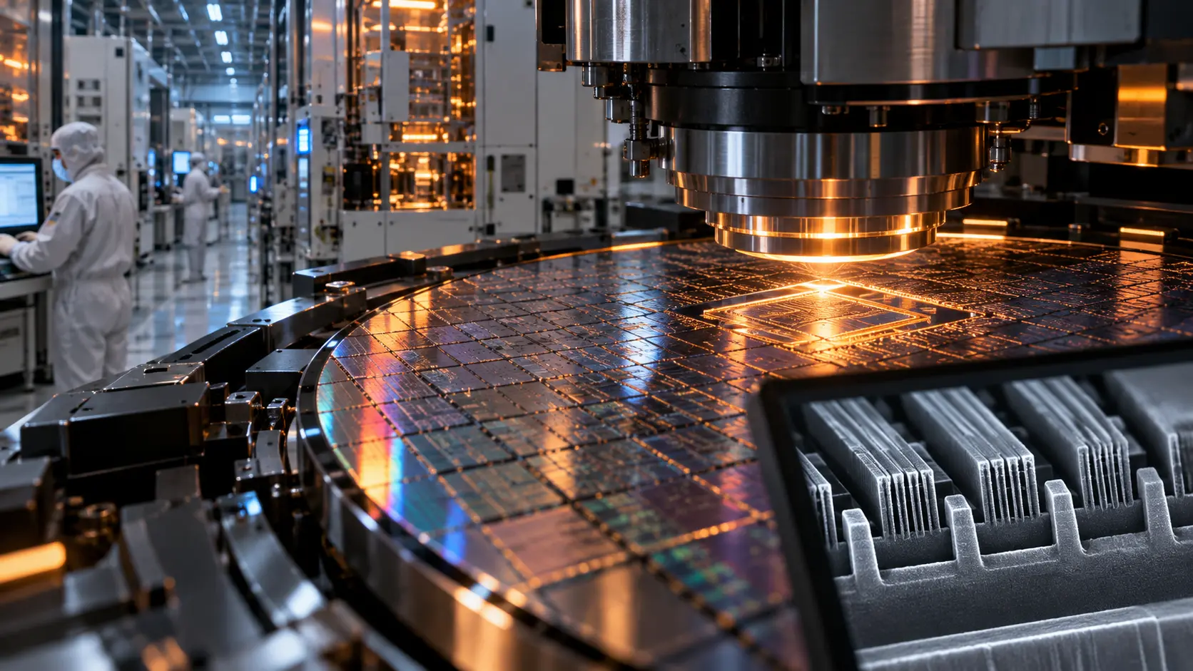
For decades, the progress of computing was closely associated with a simple trend: semiconductor manufacturers kept placing more transistors on each generation of computer chips. Smaller transistors made it possible to build processors that were faster, more capable, and often cheaper per unit of computation. This trend became known as Moore's Law, after Intel co-founder Gordon Moore observed in the 1960s that the number of components on integrated circuits was increasing at a remarkably regular pace. Moore's Law was never a physical law, but it became an influential description of how rapidly semiconductor technology was advancing.
Today, that pattern is under increasing pressure. Transistors are still becoming smaller, and leading manufacturers continue to develop more advanced fabrication processes, but the improvements are harder and more expensive to achieve. The semiconductor industry is approaching physical, engineering, and economic limits that make traditional scaling far less straightforward than it once was. Rather than signaling the end of progress, however, the slowdown is changing the way computer chips are designed.
The basic logic behind Moore's Law was closely connected to transistor scaling. A transistor acts as a tiny electronic switch. Billions of these switches can be combined to perform calculations, store information, and control the movement of data inside a processor. When manufacturers learned to make transistors smaller, they could fit more of them into the same area of silicon. Smaller devices could also switch more quickly and, for many generations, consume less energy per operation.
This combination created extraordinary improvements. Processor performance increased rapidly while computing became less expensive. Personal computers, smartphones, cloud computing, digital cameras, modern vehicles, and artificial intelligence all benefited from the semiconductor industry's ability to manufacture increasingly dense integrated circuits.
The problem is that shrinking a transistor becomes much more difficult when its dimensions approach the scale of only a few nanometers. At these sizes, effects that were once relatively minor become major engineering obstacles. Electrons can behave in ways that make it harder to control whether a transistor is fully on or off. Leakage currents can increase, and small variations in manufacturing can have a larger effect on device behavior.
Quantum mechanical effects also become increasingly relevant. One example is quantum tunneling, in which electrons can pass through barriers that would prevent them from crossing in a larger conventional device. Semiconductor engineers have developed increasingly sophisticated structures and materials to control these effects, but each new generation requires more complex solutions.
Heat presents another fundamental problem. Increasing transistor density does not automatically mean a chip can use all of its transistors at maximum power simultaneously. Modern processors can generate substantial heat, and removing that heat becomes increasingly difficult as more computation is concentrated into a small area. Excessive temperatures can reduce efficiency, damage components, or force processors to operate at lower speeds.
This challenge became especially important when traditional frequency scaling slowed. For many years, processor manufacturers could improve performance partly by increasing clock speeds. Eventually, higher frequencies produced too much power consumption and heat. The industry responded by adding multiple processor cores rather than relying solely on faster individual cores. That transition was an early sign that simple transistor scaling was no longer enough to guarantee straightforward performance improvements.
The economics of semiconductor manufacturing have changed just as dramatically as the physics. Producing leading-edge chips requires some of the most sophisticated industrial equipment ever created. Modern fabrication plants cost enormous amounts to build, and the machines used to create extremely small circuit features are highly complex. Advanced lithography, materials engineering, process control, inspection, and packaging all add to manufacturing costs.
Design costs have also risen. A smaller fabrication process may allow engineers to fit more transistors onto a chip, but creating a sophisticated processor with tens of billions of transistors requires enormous engineering teams, advanced design software, extensive verification, and increasingly complex intellectual property. Not every company or product can justify moving to the newest manufacturing node.
This economic reality changes one of the original assumptions associated with Moore's Law. Historically, shrinking transistors tended to reduce the cost of each transistor. Today, the newest manufacturing processes can provide important performance and density improvements, but those benefits come with much higher development and manufacturing expenses. A cutting-edge transistor is no longer guaranteed to become dramatically cheaper simply because it is smaller.
This is why asking whether Moore's Law is "dead" can produce different answers. If Moore's Law means that transistor density can continue increasing indefinitely at roughly the historical rate while the cost per transistor consistently declines, that model is clearly under strain. If it simply means that engineers will continue finding ways to place more computing capability into advanced systems, the trend has not ended. Instead, the methods are changing.
One major response is specialization. Rather than expecting a general-purpose CPU to perform every type of computation efficiently, designers increasingly build specialized processors for particular workloads. Graphics processing units are one prominent example. GPUs contain large numbers of processing units designed for parallel workloads, making them useful not only for graphics but also for scientific computing and artificial intelligence.
AI accelerators take specialization even further. Neural networks depend heavily on operations such as matrix multiplication, and chips designed specifically for these workloads can perform them more efficiently than general-purpose processors. Specialized video processors, networking accelerators, cryptographic engines, and signal-processing units follow the same principle. Performance improvements increasingly come from designing hardware around the problem rather than merely making every transistor smaller.
This change is particularly important because energy efficiency has become a major constraint. A specialized accelerator can eliminate unnecessary circuitry and optimize data movement for a particular task. It may therefore produce much more useful work for each watt of electricity consumed. In data centers, where power and cooling are major expenses, these improvements can be economically significant.
Another major development is the use of chiplets. Traditional processors were often designed as single large pieces of silicon containing most of the system's functions. As chips became larger and more complicated, this approach became increasingly expensive. Large dies are harder to manufacture without defects, and producing every component using the most advanced process may be unnecessary.
Chiplet architectures divide a processor into several smaller pieces that are connected inside the same package. One chiplet might contain CPU cores, another could manage input and output, while others could provide memory interfaces or specialized accelerators. Different components can even be manufactured using different semiconductor processes according to their requirements.
This modular approach offers several advantages. Smaller dies can improve manufacturing yields because a defect destroys a smaller piece of silicon rather than an enormous processor. Designers can reuse chiplets across multiple products, potentially reducing development costs. They can also reserve expensive leading-edge fabrication for components that benefit most from it while producing less demanding functions on older, cheaper processes.
The challenge is connecting these chiplets efficiently. Data moving between separate pieces of silicon can consume more energy and experience greater delays than data traveling within a single chip. Advanced packaging and high-speed interconnect technologies are therefore becoming essential parts of processor design. The package itself is increasingly becoming part of the computing architecture rather than merely a protective container around the chip.
Three-dimensional integration takes this idea further by stacking components vertically. Traditional chips primarily expand across a flat silicon surface. A 3D design places layers of circuitry or memory on top of one another, potentially reducing the physical distance that data must travel and increasing the amount of functionality that can fit into a given area.
Memory technology is especially important in this transition. Many modern workloads are limited not by how quickly processors can perform arithmetic but by how quickly they can access data. Moving information between a processor and distant memory consumes both time and energy. Bringing memory closer to computing units through advanced packaging or vertical stacking can improve performance without relying solely on smaller transistors.
This issue is particularly visible in artificial intelligence. Large AI models require enormous amounts of data to move continuously between memory and processing units. A chip may contain extremely powerful arithmetic hardware, but that hardware cannot operate at full capacity if it is constantly waiting for data. As a result, memory bandwidth and interconnect performance are becoming as important as the speed of the processing cores themselves.
New transistor designs are also extending traditional semiconductor scaling. As conventional planar transistors became difficult to control at small dimensions, manufacturers adopted three-dimensional structures that give the gate greater control over the electrical channel. Successive generations continue to modify transistor geometry and materials in an effort to improve performance and reduce leakage.
These innovations show that semiconductor limits are not a single wall that the industry suddenly reaches. Engineers encounter particular constraints and then redesign devices to work around them. Some solutions extend transistor scaling, while others change the architecture of the entire computing system. Progress increasingly depends on several technologies advancing together.
The materials used in chips may also evolve. Silicon remains the foundation of mainstream computing because the semiconductor industry has developed an enormous manufacturing infrastructure around it. However, researchers continue investigating new materials and device structures that could complement or eventually replace silicon for specific applications. The challenge is not simply proving that a new material works in a laboratory but manufacturing billions of reliable devices at commercially viable cost.
Software is also becoming more important as hardware grows more heterogeneous. A computer containing CPUs, GPUs, AI accelerators, and other specialized processors must decide which workload should run on each component. Developers need programming tools, compilers, operating systems, and frameworks capable of using this hardware efficiently. Hardware specialization can deliver enormous gains, but those gains disappear if software cannot take advantage of the underlying architecture.
This represents a major shift from an earlier era of computing. When processor performance increased rapidly from one generation to the next, software developers could often rely on future hardware to make programs faster. As automatic improvements from transistor scaling weaken, programmers and hardware designers must work more closely together. Better algorithms, parallelism, specialized accelerators, and efficient data movement become increasingly important.
The end of easy scaling also affects competition within the semiconductor industry. Building leading-edge fabrication facilities has become so expensive and technologically demanding that relatively few companies can manufacture the most advanced chips. At the same time, chiplet designs and specialized accelerators can allow other companies to innovate without manufacturing every component themselves. Semiconductor competition is therefore moving beyond transistor size toward architecture, packaging, software, memory, and complete system design.
For consumers, this change may make progress appear less uniform than it once did. A new processor may not be dramatically faster than its predecessor in every application. Instead, it may deliver large improvements in specific workloads, better energy efficiency, stronger AI performance, faster graphics, or more effective integration with specialized hardware. Computing progress is becoming more dependent on what the computer is being asked to do.
Moore's Law is therefore better understood as entering a new phase than simply ending. The semiconductor industry can no longer depend on shrinking conventional transistors to provide every improvement automatically. Physical effects, heat, manufacturing complexity, and rising costs have made that strategy increasingly difficult. Yet demand for more computing power continues to drive innovation.
The future of computer chips will rely on a combination of smaller and more sophisticated transistors, specialized processors, chiplets, three-dimensional integration, advanced packaging, faster memory systems, and better software coordination. Improvements may arrive through several architectural changes at once rather than through a predictable doubling of transistor density.
The most important consequence of the semiconductor limits now emerging is therefore not the end of computing progress. It is the end of an era in which one dominant technique could drive that progress almost by itself. Future computers will improve by becoming more specialized, more modular, and more tightly integrated, shifting the focus from simply making transistors smaller to designing entire computing systems more intelligently.
