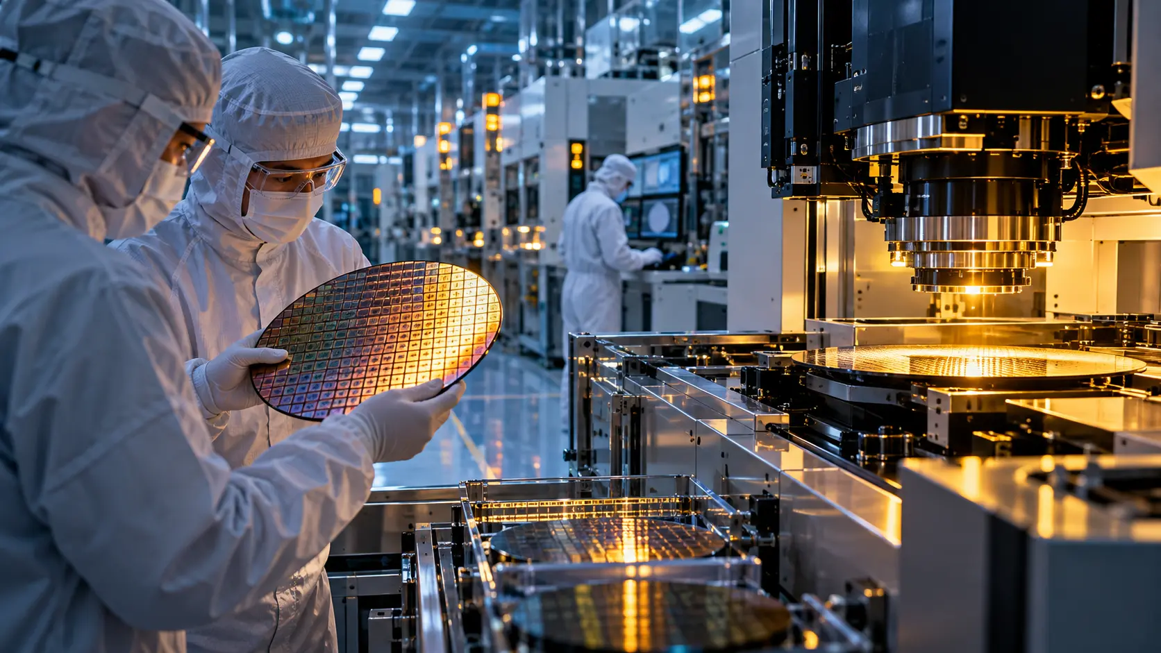
Modern computer chips contain billions of microscopic electronic components packed into an area that can fit on a fingertip. They power smartphones, computers, cars, data centers, medical devices, communication systems, and countless other technologies. Producing them requires far more than simply assembling tiny parts. The semiconductor manufacturing process combines advanced circuit design, materials science, chemistry, optics, physics, precision machinery, and extremely controlled factory environments. A modern chip is built through hundreds or even thousands of carefully coordinated operations, many of which must work at scales measured in nanometers.
The process begins long before any physical chip exists. Engineers first design the electronic circuits that will eventually be created on silicon. A processor, for example, may contain billions of transistors connected through a complex network of microscopic wires. Transistors act as extremely small electronic switches, controlling electrical signals and allowing the chip to perform calculations, store information, and execute instructions. Engineers use specialized software known as electronic design automation tools to design these circuits, simulate their behavior, verify that they function correctly, and determine how the components should be arranged on the chip.
Chip design is divided into many stages because the complexity is far beyond what engineers could manage manually. Designers define the chip's overall architecture, determine how its major functional blocks communicate, create digital logic, arrange components physically, and design the network of electrical connections between them. Software continuously checks for problems such as incorrect connections, timing errors, excessive power consumption, or layouts that cannot be manufactured reliably. Once the design has passed extensive verification, its physical patterns are prepared for the manufacturing equipment that will reproduce them on silicon.
Silicon is the foundation of most modern chips because of its useful electrical properties and its abundance. Pure silicon behaves differently from both a normal conductor, such as copper, and an insulator, such as glass. It is a semiconductor, meaning its ability to conduct electricity can be carefully controlled. By adding tiny quantities of other elements to silicon, manufacturers can change its electrical behavior and create the regions needed to form transistors.
Chip manufacturing starts with extremely pure silicon. The material is processed into a large single crystal, which is then sliced into thin, circular discs called wafers. These wafers are polished until their surfaces are extraordinarily smooth and flat. A single wafer can eventually contain hundreds or even thousands of individual chips, depending on the size of the wafer and the dimensions of each chip.
The wafer then enters a semiconductor fabrication plant, often called a fab. Inside these facilities, contamination must be controlled with extraordinary care. A tiny particle of dust can be enormous compared with the microscopic features of a modern transistor and may destroy part of a circuit. Manufacturing therefore takes place in cleanrooms where air is continuously filtered and workers wear protective clothing designed to prevent skin particles, hair, fibers, and other contaminants from reaching the wafers.
One of the most important techniques in the semiconductor manufacturing process is photolithography. Photolithography transfers microscopic circuit patterns onto the wafer. First, the wafer is coated with a light-sensitive material called photoresist. A lithography machine then exposes selected areas of this coating to light according to the circuit pattern being manufactured. After chemical development, parts of the photoresist remain while other parts are removed, leaving a temporary pattern on the wafer.
The patterns used in modern chips are so small that producing them requires exceptionally sophisticated optical systems. Advanced manufacturing processes use extreme ultraviolet lithography, commonly called EUV, for some of the most demanding layers. EUV systems use light with a very short wavelength, allowing manufacturers to create extremely small features. Producing, controlling, and focusing this light is technically difficult, and the machines rely on highly specialized mirrors, vacuum systems, light sources, sensors, and precision controls.
Lithography does not create the entire chip in a single step. Instead, it defines where other manufacturing processes should modify the wafer. After a pattern has been created, manufacturers may remove material through a process called etching. Depending on the step, gases or chemicals selectively remove exposed regions while protected areas remain intact. The accuracy of this process is critical because even very small deviations can affect the electrical performance of the resulting transistors.
Other steps add materials rather than remove them. Semiconductor manufacturing uses several deposition techniques to place extremely thin films on the wafer. These films can act as conductors, insulators, protective barriers, or functional parts of transistors. Some deposited layers may be only a few atoms thick. Methods such as chemical vapor deposition, physical vapor deposition, and atomic layer deposition are used depending on the material and the precision required.
Manufacturers must also control the electrical properties of the silicon itself. One important technique is ion implantation, in which electrically charged atoms are accelerated toward the wafer and embedded in carefully selected regions. This changes how those regions conduct electricity. Combined with other processes, such modifications help form the structures that allow individual transistors to switch between electrical states.
These operations are repeated again and again. A modern chip is not a flat circuit printed once on a piece of silicon. It is a complex three-dimensional structure built through many layers. Some layers create the transistors themselves, while others form the microscopic electrical connections that link billions of components together. Insulating materials separate conductive paths so signals can travel through the chip without interfering with one another.
Between many manufacturing stages, the wafer must be made flat again. Chemical mechanical polishing is commonly used for this purpose. The process combines chemical reactions with mechanical polishing to remove excess material and create a smooth surface for the next layer. Maintaining flatness is essential because later lithography steps must focus accurately across the wafer.
Alignment is another major challenge. Each new layer must be positioned extremely precisely in relation to the layers already below it. If patterns are shifted too far, electrical connections may fail or transistors may not work correctly. Manufacturing equipment therefore uses advanced measurement and positioning systems to monitor the wafer and control each operation with microscopic precision.
The environment surrounding the manufacturing process is equally important. Temperature, humidity, vibration, chemical purity, airflow, and electrical conditions must all be carefully controlled. Even small variations can influence the dimensions or properties of structures being manufactured. Semiconductor fabs therefore contain extensive systems for delivering purified water, specialized gases, chemicals, electricity, and tightly controlled air.
Throughout production, manufacturers inspect and measure the wafers. Specialized instruments look for defects, check whether features have the correct dimensions, and confirm that layers are properly aligned. Because the structures can be smaller than the wavelengths of visible light, ordinary optical microscopes are not always sufficient. Manufacturers use advanced imaging and measurement technologies to examine features and identify potential problems.
Not every chip on a wafer survives the process perfectly. Small defects can cause individual chips to fail even when most of the wafer is usable. The percentage of functional chips produced from a wafer is known as yield. High yield is economically crucial because semiconductor fabrication is extremely expensive. Manufacturers continually adjust equipment and production conditions to reduce defects and increase the number of usable chips.
Once wafer fabrication is complete, each chip is electrically tested. The wafer is then cut into individual pieces called dies. Functional dies move on to packaging, where they are placed in protective structures that provide electrical connections to the outside world and help manage heat. Modern packaging can itself be highly sophisticated, especially when several dies, memory components, or specialized processors are combined within a single package.
The finished chips undergo additional testing to confirm that they operate correctly at different voltages, temperatures, and workloads. Chips from the same manufacturing batch may also perform somewhat differently. Manufacturers can test and classify them according to factors such as operating frequency, power consumption, or the number of functional processing units before they are sold for particular products.
The extraordinary complexity of chip manufacturing explains why semiconductor factories require enormous investment. A leading-edge fab contains some of the most advanced industrial equipment ever built. Lithography systems, deposition equipment, plasma etchers, inspection instruments, chemical processing systems, and automated wafer-handling machines must operate together with exceptional reliability. Building and equipping an advanced fabrication plant can require investments measured in many billions of dollars.
The supply chain behind these factories is equally specialized. Chip manufacturers depend on companies that produce manufacturing equipment, ultra-pure chemicals, silicon wafers, specialty gases, optical systems, photoresists, packaging materials, design software, and many other technologies. Some of these products require decades of accumulated expertise and cannot easily be replaced by ordinary industrial alternatives.
Manufacturing difficulty also increases as engineers try to place more computing capability into smaller areas. Smaller features can improve performance and energy efficiency, but they also make defects, electrical interference, heat, and manufacturing variation harder to control. Modern transistor structures have therefore become increasingly sophisticated, moving beyond simple planar designs toward three-dimensional architectures that provide better control over electrical current.
This combination of scale and precision makes the semiconductor manufacturing process unusual among industrial activities. Manufacturers must produce enormous quantities of chips while controlling structures that are almost unimaginably small. Chemical reactions, optical exposure, material deposition, etching, polishing, measurement, and electrical testing must all work within extremely tight limits, repeatedly, across many layers and many wafers.
A finished processor may look like a small and relatively simple object, but it is the result of an immense technological system. Its billions of transistors begin as a digital design and gradually become physical structures through repeated cycles of lithography, material deposition, etching, modification, polishing, and inspection. The need to perform these operations at nanometer scales, with exceptionally low defect rates and perfect coordination between hundreds of manufacturing stages, is what makes modern chip production one of the most complex industrial processes in the world.